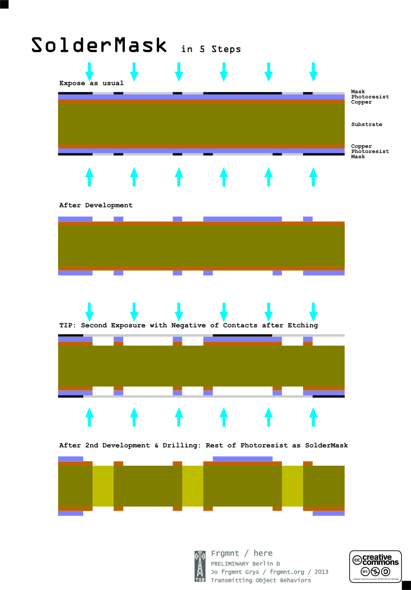
Here I show your how to integrate some new steps in your photographic PCB-production process.
After the usual step of exposure with a positive of your track patterns & development & etching you just add another exposure with a negative of your solder mask pattern. As a result you get the rest of the etch resist as solder mask to stay on your PCB as protection & solder repellent. The idea comes from a Bungard datasheet.

